EECS 31/CSE 31/ICS 151 Homework 6 Questions with Solutions
View Questions Only
View Questions with Strategies
Problem 1
Question
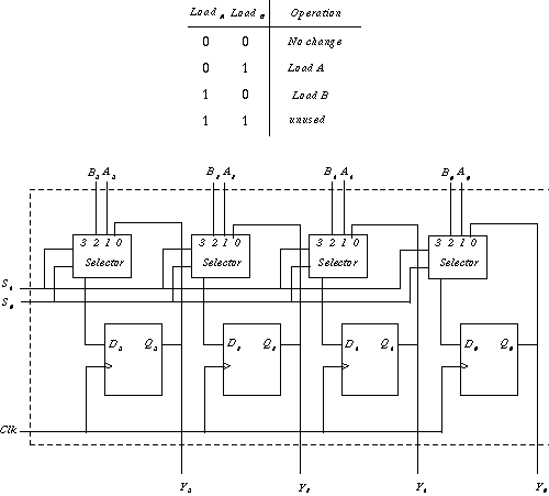
(Registers) Design a register with two load signals, that enable the loading of data from two different sources.
Solution
Problem 2
Question
(Shift-Registers) Using a 4-bit shift register, construct a 4-bit register that can rotate its content one position to the left or right.
Solution
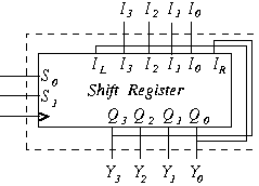
Logic Schematic
Problem 3
Question
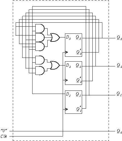
(Counters) Design a 4-bit binary counter that counts up only in:
- Even numbers (0, 2, 4, 6, 8, ...)
Solution
-
Develop state/output table.
PRESENT STATE NEXT STATE Q3 Q2 Q1 Q0 Q3(next) Q2(next) Q1(next) Q0(next) 0 0 0 0 0 0 1 0 0 0 1 0 0 1 0 0 0 1 0 0 0 1 1 0 0 1 1 0 1 0 0 0 1 0 0 0 1 0 1 0 1 0 1 0 1 1 0 0 1 1 0 0 1 1 1 0 1 1 1 0 0 0 0 0 -
Write the next-state equations.
 Q3(next) = Q3Q1' + Q3Q2' + Q3'Q2Q1
 Q2(next) = Q2Q1' + Q2'Q1
 Q1(next) = Q1'
 Q0(next) = 0
-
Draw logic schematic.
Problem 4
Question
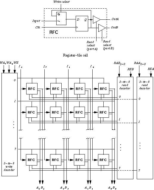
(Register files) Design an 8 x 4 register file with:
- One write and two read ports
Solution
Problem 5
Question
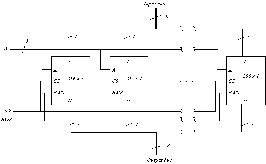
(Memories) Design:
- 256K x 8 RAM using 256K x 1 RAM chips
Solution
Problem 6
Question
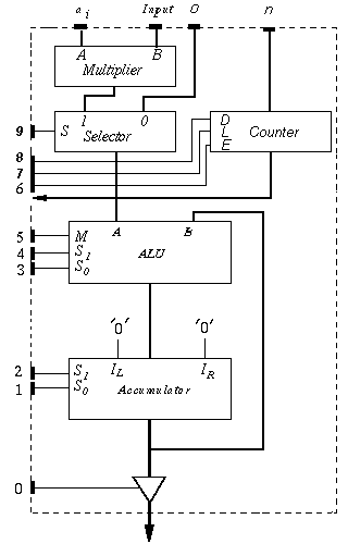
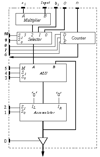
(Datapaths) Design a simple datapath that can compute the expression:
 aixi
aixi aixi + bi
Solution
Problem 7
Question
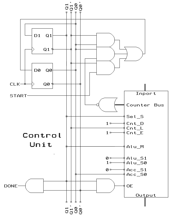
(Datapaths) Define and implement the controller for the datapath that couldexecute the algorithm developed in Problem 7.19(a).
Solution
-
Write out the basic algorithm.
sum := 0 loop: for i = 1 to n sum := sum + aixi end loop output := sum - Assign the vaiable to the registers. Here ai and xi and are inputs, don't need extra registers to store them, we use couter to store n, accumulator to store sum.
-
Derive the proper control word for each statement.
Selector
(S)Counter
(D L E)ALU
(M S1 S0)Accumulator
(S1 S0)Output
(OE)0 x 1 x 0 0 1 0 1 0 1 1 0 1 1 0 1 0 1 0 x x x x 0 0 0 0 0 1 -
Develop state diagram (FSM representation) for the above algorithm.
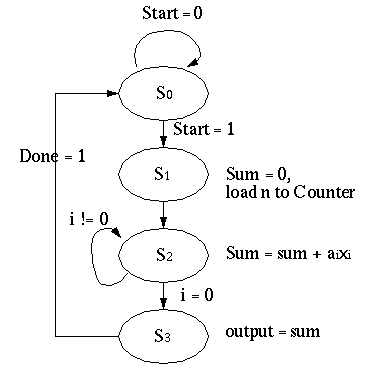
-
Draw next-state table, write next-state equations.
STATES Q1Q0 Start, (i = 0) 00 01 11 10 S0 00 00 00 01 01 S1 01 11 11 11 11 S2 11 11 10 10 11 S3 10 00 00 00 00 Q1(next)Q0(next) Q1(next) = Q0 Q0(next) = Q1'Q0 + Q0(i = 0)' + Q1'Start
-
Draw output logic table, write output equations.
STATE Q1Q0 Selector
(S)Counter
(D L E)ALU
(M S1 S0)Accumulator
(S1 S0)Output
(OE)S0 00 x x x x x x x x x x 0 S1 01 0 1 0 1 1 0 1 0 1 0 S2 11 1 1 0 1 1 0 1 0 1 0 S3 10 x x x x x x x 0 0 1 Sel_S = Q1 Cnt_D = 1 Cnt_L = Q1' Cnt_E = 1 Alu_M = Q1 Alu_S1 = 0 Alu_S0 = 1 Acc_S1 = 0 Acc_S0 = Q0 OE = Q1Q0'
-
Develop logic schematic.
