EECS 31/CSE 31/ICS 151 Homework 4 Questions with Solutions
View Questions Only
View Questions with Strategies
Problem 1
Question
(Adders) Design a 2-bit adder slice that will combine the functions of two FAs. Using the library presented in Table 3.14, compare the delay of your design with that of the design shown in Figure 5.1.
- Write out sum and carry equations for S1, S2 and C1, C2 from X2, Y2, X1, Y1 and C0.
- Substitude C1 in S2 and C2 equations with its correspondent expression.
- Draw the correspondent logic schematic with AND, OR and XOR gates.
- Compute input/output delays.
Solution
-
Write out sum and carry equations,
S0 = X0 Y0
Y0  C0
C0
C1 = X0Y0 + C0(X0 Y0)
Y0)
S1 = X1 Y1
Y1  C1
C1
C2 = X1Y1 + C0(X1 Y1)
Y1)
-
Substitude C1 in S2 and C2 equations with its correspondent expression,
S1 = X1 Y1
Y1  (X0Y0 + C0(X0
  Y0))
Y0))
C2 = X1Y1 + (X0Y0 + C0(X0 Y0))(X1
  Y1)
Y1)
Extend C2 expression,
C2 = X1Y1 + X0Y0(X1 Y1) + C0(X0
  Y0)(X1
  Y1)
Y1)
-
Draw the logic schematic with NAND, OR and XOR,
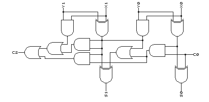
-
Compute the input/output delays,
S0 is 8.4, S1 is 13.2, and C2 is 11.4.
Problem 2
Question
(Carry-look-ahead generators) Design a 64-bit CLA adder, using:
- One level of CLA
- Two levels of CLA
- Three levels of CLA
Solution
-
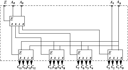
Let a 4 bit single level CLA adder be represented by
The single level of 64-bit CLA adder can be implemented by chaining these 4-bit single level CLA adders as shown below: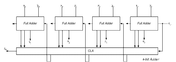

-
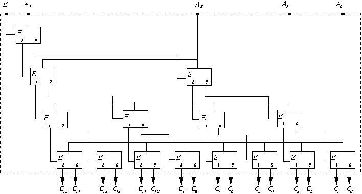
To design a 64-bit adder with two levels of CLA, we can chain the 16-bit two level CLA adder together. A 16-bit two level CLA adder can be represented by
Giving us the final implementation below: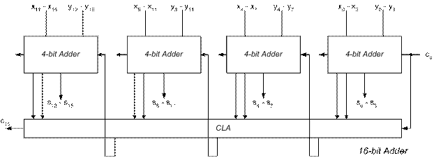
Or you can use the 16-bit one level CLA adder, connecting them by CLA, as shown below:
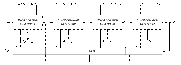
-
To design a 64-bit adder with three levels of CLA, we can use the 16-bit two level CLA adder given in (b), connecting 4 16-bit two level CLA adders with single level CLA generator, giving us the final implementation below:
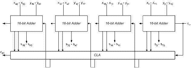
Problem 3
Question
(Logic units) Design a logic unit that will perform the following combinations of operations.
- NAND, NOR, transfer, and complement
- XOR and XNOR
Solution
-
(1) & (2) Develop truth table and assign one group of S1, S0 values per function.
x y NOR NAND Transfer NOT S1S0 = 00 S1S0 = 01 S1S0 = 11 S1S0 = 10 0 0 1 0 0 1 0 1 1 0 0 1 1 1 0 1 1 0 1 0 1 0 1 0 (3) Write the Boolean expression and convert it into standard sum-of-product form.
S0'x' + S1'S0'y' + S0xy + S1S0x(4) Draw logic schematic for the Boolean expression.
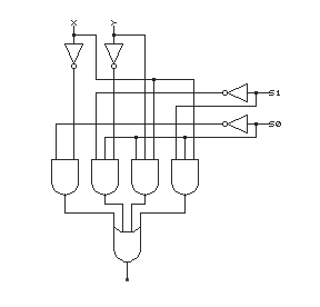
-
(1) & (2) Develop truth table and assign one value of S per function.
x y XOR XNOR (S = 0) (S = 1) 0 0 0 1 0 1 1 0 1 1 0 1 1 0 1 0 (3) Write the Boolean expression and convert it into standard sum-of-product form.
Sx'y' + S'x'y + Sxy + S'xy'(4) Draw logic schematic for the Boolean expression.
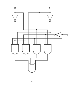
Problem 4
Question
(ALUs) Design an ALU that can perform add, subtract, NAND, and NOR operations.
Solution
-
Draw truth table for AE and LE,
Truth table for AE:
   M  |  S0  |  Yi
 -------------------
   1  |  0   |  bi
   1  |  1   |  bi'
Truth table for LE:
   M  |  S0  |  Xi
 -----------------------
   0  |  0   |  (aibi)'
   0  |  1   |  (ai+bi)'
   0  |  x   |  ai
-
Write Boolean expressions for AE and LE,
 Yi = MS0'bi + MS0bi'
 Xi = Mai + M'S0'(aibi)' + M'S0(ai + bi)'
-
Draw logic schematic from the above boolean expression for AE and LE,

 Cost  = 26                         |         Cost  = 42
 Delay = 6.2ns                      |         Delay = 7ns
If we use K-Maps, for the LE, we can do as following:
-
Draw K-Maps according to the LE truth table
Truth table for LE:
   M  |  S0  |  Xi
 -----------------------
   0  |  0   |  (aibi)'
   0  |  1   |  (ai+bi)'
   0  |  x   |  ai
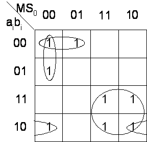
-
Get the minimal cover set from the K-Map
Xi = Mai + M'S0'ai' + M'ai'bi' + S0'aibi'
-
Draw the logic schematic from the above boolean expression for LE
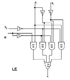
 Cost  = 48
 Delay = 7ns
Problem 5
Question
(Decoders) Design a 4-to-16 decoder, using:
- 1-to-2 decoders
- 2-to-4 decoders
Solution
Problem 6
Question
(Comparators) Design the serial and parallel verions of a comprator that can compare the following types of number representation.
- Sign-magnitude
- Two's complement
- Floating point
Solution
(a) and (c):
The two numbers to be compared are X and Y, let Sx represent the sign bit of X, Mx represent the magnitude (exponent and mantissa) of X, Sy represent the sign bit of Y, My represent the magnitude (exponent and mantissa)of Y, G0, L0 represent the magnitude outputs, G1, L1 represent the final outputs.
-
Develop truth table from the algorithm.
Sx Sy G0 L0 G1 L1 0 0 0 0 0 0 0 0 0 1 0 1 0 0 1 0 1 0 0 0 1 1 0 0 0 1 0 0 1 0 0 1 0 1 1 0 0 1 1 0 1 0 0 1 1 1 1 0 1 0 0 0 0 1 1 0 0 1 0 1 1 0 1 0 0 1 1 0 1 1 0 1 1 1 0 0 0 0 1 1 0 1 1 0 1 1 1 0 0 1 1 1 1 1 0 0 -
Write the Boolean expressions, convert them into standard form.
 G1 = Sx'Sy + Sx'G0L0' + SyG0'L0
 L1 = SxSy' + Sy'G0'L0 + SxG0L0'
- Develop logic schematic and connect magnitude comparator with the logic schematic.
-
For the magnitude comparator, you can use serial or parallel design (pg. 196 on textbook)
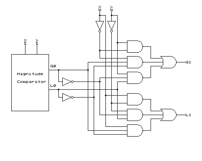
(b)Two's complement:
The two numbers to be compared are X and Y, let Sx represent the MSB of X, Mx represent the other bits of X, Sy represent the MSB of Y, My represent the other bits of Y, G0, L0 represent the magnitude outputs, G1, L1 represent the final outputs.
-
Develop truth table from the algorithm.
Sx Sy G0 L0 G1 L1 0 0 0 0 0 0 0 0 0 1 0 1 0 0 1 0 1 0 0 0 1 1 0 0 0 1 0 0 1 0 0 1 0 1 1 0 0 1 1 0 1 0 0 1 1 1 1 0 1 0 0 0 0 1 1 0 0 1 0 1 1 0 1 0 0 1 1 0 1 1 0 1 1 1 0 0 0 0 1 1 0 1 0 1 1 1 1 0 1 0 1 1 1 1 0 0 -
Write the Boolean expressions, convert them into standard form.
 G1 = Sx'Sy + Sx'G0L0' + SyG0L0'
 L1 = SxSy' + SxG0'L0 + Sy'G0'L0
- Develop logic schematic and connect magnitude comparator with the logic schematic.
-
For the magnitude comparator, you can use serial or parallel design (pg. 196 on textbook)
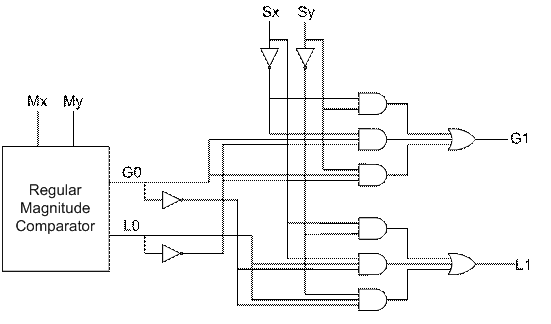
Problem 7
Question
(Shifters) Design an 8-bit barrel:
- Left rotator
- Left shifter
- Left and right shifter
- Left and right shifter/rotator
Solution
-
Left rotator
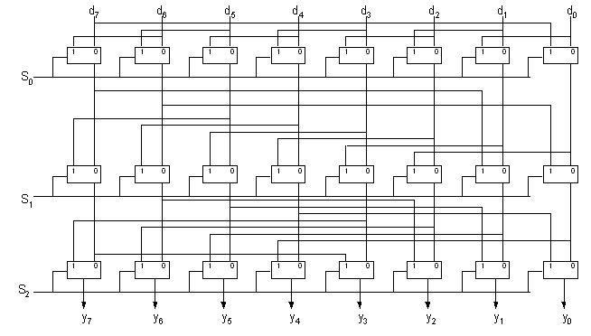
-
Left shifter
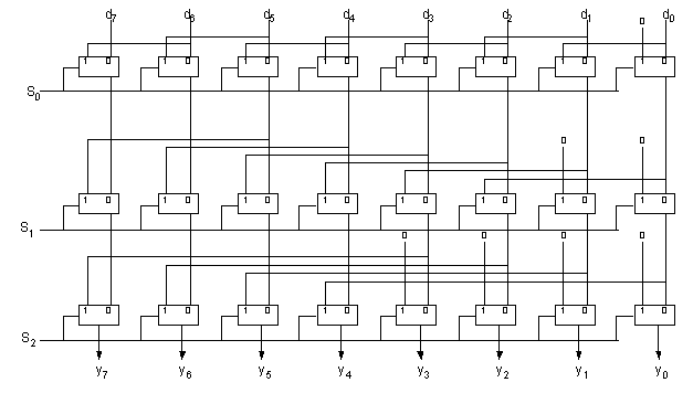
-
Left and right shifter
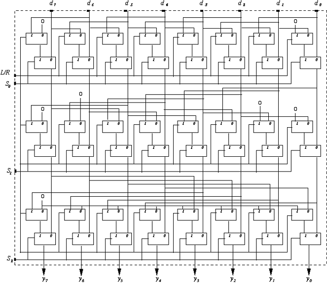
-
Left and right shifter/rotator
The solution given below only displays the first layer
Problem 8
Question
(ROMs) Using a 16x4 ROM, implement a 2-bit comparator that can generate "greater than," "less than," and "equal to" functions.
Solution
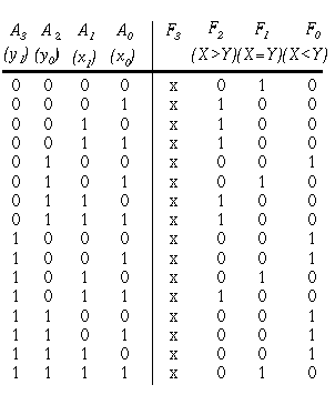
Truth Table
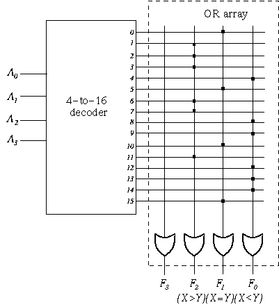
ROM Program
Design Synthesis Example
Question
Design a Polite & Stupid Elevator
Assumptions:
- There are three floors
- Door opens on every floor
- One button at any time
Solution
-
We assume there are 5 states as shown below. The inputs to the state diagram are the Button 1, 2, 3 or no button pressed. F1, F2 and F3 represent the elevator's destination is 1, 2, 3 floor. F2D represent the elevator passing floor 2 when it goes down from third floor to first floor without pressing Button 2. F2U represent the elevator passing floor 2 when it goes up from first floor to third floor without pressing Button 2. The outputs of this state diagram are directions of the elevator, which indicating the elevator is going up or going down.
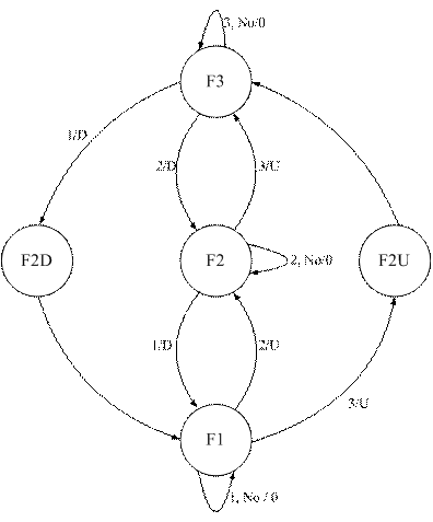
-
Based on the above state diagram, we can get the next-state table on different button inputs:
Present State Next State Button 1 Button 2 Button 3 No Button F1 F1 F2 F2U F1 F2 F1 F2 F3 F2 F2U F3 F3 F3 F3 F2D F1 F1 F1 F1 F3 F2D F2 F3 F3 We encode these 5 states with F1 = 010, F2 = 100, F2U = 001, F2D = 000, F3 = 110. Then we can represent these 5 states by using three D flip-flops. Let Q2, Q1, and Q0 represent the outputs of these D flip-flops. For the input button, we use B1, B0 to represent which button is pressed. Hence, the above table can be transformed to:
Present State Next State Button 1 Button 2 Button 3 No Button Q2Q1Q0 B1B0 = 01 B1B0 = 10 B1B0 = 11 B1B0 = 00 F1 = 010 F1 = 010 F2 = 100 F2U = 001 F1= 010 F2 = 100 F1 = 010 F2 = 100 F3 = 110 F2 = 100 F2U = 001 F3 = 110 F3 = 110 F3 = 110 F3 = 110 F2D = 000 F1 = 010 F1 = 010 F1 = 010 F1 = 010 F3 = 110 F2D = 000 F2 = 100 F3 = 110 F3 = 110 -
We can draw the K-maps for the next-state table as following. There are 5 variables, the output of the 3 D flip-flops Q2, Q1, and Q0 and the input button B1, B0. Each value in a square represent the next-state value corresponding to the next-state table. For those square not defined in the next-state table, we use an 'X' to indicating a "don't care" occasion.

Replacing F1, F2, F3, F2U and F2D with the values of Q2, Q1, and Q0, we can get 3 K-Maps for Q2(next), Q1(next) and Q0(next), as shown below:

Q2(next) = Q0 + Q2B1 + Q2B0' + Q1B1B0'
Q1(next) = Q2'Q1' + Q2'B1' + Q1B1'B0' + Q2B1B0 + Q2Q1'B0
Q0(next) = Q2'Q1B1B0 -
Similarly, we can get the output equations based on the following K-Maps:

Down = Q2'Q1'Q0' + Q2B1'B0 + Q2Q1B1B0'
Up = Q0 + Q2'Q1B1 + Q2Q1'B1B0 -
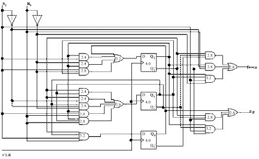
Finally, we can draw the schematic based on the next-state and output equations:
